This website uses cookies so that we can provide you with the best user experience possible. Cookie information is stored in your browser and performs functions such as recognising you when you return to our website and helping our team to understand which sections of the website you find most interesting and useful.
Vyhledávání
Energy-dispersive X-ray spectroscopy (EDS)
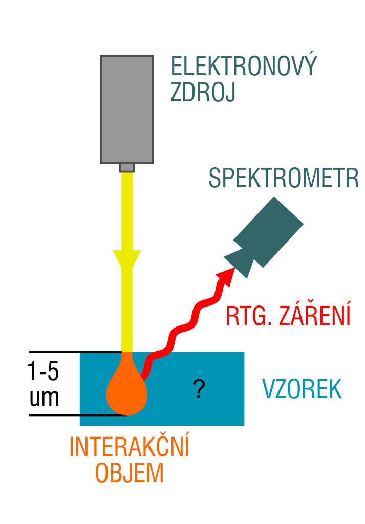
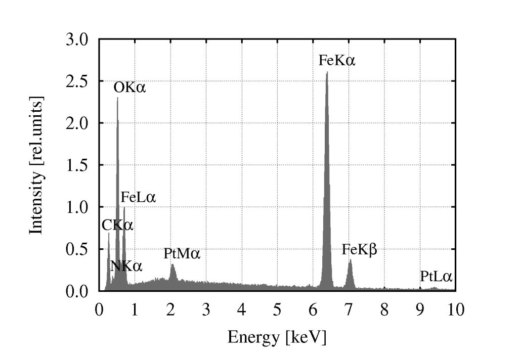
Energy-dispersive X-ray spectrometry (EDS) is an analytical method based on the detection of characteristic X-rays emitted in the interactions between an electron beam and the surface of the sample. From energies of the photons emitted in these interactions, we obtain the EDS spectrum that enables us to determine individual constituent elements of the sample, as well as their quantities, that is, their chemical composition.
Characteristic of the EDS is its use of solid-state silicon detectors, where the impact of X-rays or photons generates electron-hole pairs. Their number is proportionate to the energy of the photon. We obtain the EDS spectrum by amplifying and processing the pulses. The measurement itself is very fast, the results are available within minutes. In addition to point-based chemical analysis, where the signal stems from a very small volume of the studied material (the so called interaction volume), it is possible to scan the surface of a material using an electron beam in two dimensions, acquiring a 2D chemical map. This procedure is frequently used for every element separately for us to obtain information about its representation in a given area. The EDS detection limits are in the order of tenths of percent of a mass content for a given element in the studied material.
The same principle like that of the EDS is used in the Wavelength-dispersive X-ray spectroscopy (WDS). But unlike EDS, which analyses the whole spectrum irradiated from a material, WDS makes element-by-element assessments based on a specific wavelength given for each element. Consequently, the WDS measurements are more accurate, with smaller detection limits (in the orders of hundreds of percent of the mass content). However, this accuracy is reclaimed with not only the time spent on the job (the measurement itself takes dozens of minutes), but also with the acquisition costs associated with the device. In addition, the WDS spectrometer, working on the principle of X-ray crystal diffraction, where the crystal along with the detector is placed on the so called Rowland circle, is very large.
EDS and WDS spectrometers are typically used as auxiliary devices (detectors) for scanning (SEM) or transmission (TEM) electron microscopes. But they can also be used as separate devices.