
This website uses cookies so that we can provide you with the best user experience possible. Cookie information is stored in your browser and performs functions such as recognising you when you return to our website and helping our team to understand which sections of the website you find most interesting and useful.
Vyhledávání
Transmission electron microscope (TEM)
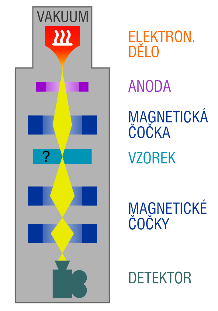
Transmission electron microscope (TEM) works on a similar principle like the scanning electron microscope (SEM). For analysing the sample, it uses an electron beam generated by a source, the so called electron gun. The beam, which like the sample is situated in a vacuum, is directed and focused on the sample using electromagnetic lenses. An important difference when compared to SEM is that we use electrons that pass through the sample to analyse the sample. This principle, that is, that the electrons are not detected until they pass through the sample is where the name “transmission” was derived from.
For this reason, a sample observed in TEM must be very thin (10 to 100 nm) for the electrons to pass through it. This enables us to analyse the internal structure of the sample. It is due to the immense magnification, enabled by the use of electrons instead of the visible light, that TEM can also show individual atoms of the sample.
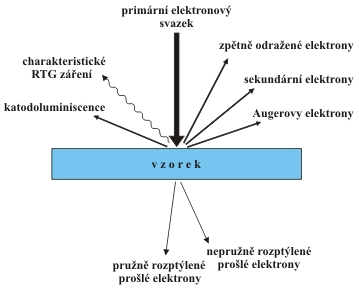
The interaction of electrons with the sample generates a variety of signals. For TEM, it is primarily electrons that passed through the sample which generate most signals, but it can also detect secondary electrons or X-rays. The most frequently used method of sample imaging is using passed-through electrons. The inelastically scattered passed-through electrons enable us to view the sample either in the bright field (BF) using an objective aperture, in the dark field (DF) using a beam tilt or using deflected electron beam as part of the STEM (scanning transmission electron microscopy) technique.
Imaging mode
For TEM imaging, the most frequently used technique is the bright field (BF) technique. It means that all sample passed-through electrons are used for creating the image. The contrasts in the image for samples with lower magnification (up to 100 000times) are a result of a weight contrast (thicker areas or heavier atoms absorb more electrons, and appear darker). For magnification higher than 200 000times, it is a phase contrast that prevails, where the main role is played by the interference of passed-through electrons on structures of the sample. This enables the atomic-scale resolution.
Another imaging option is using the so called dark field (DF), which works on the principle of the selection of electrons reflected in a chosen direction on selected atomic planes of the sample. Using dark field also enables us to increase a resolution limit of the microscope, making it possible to observe details not apparent in the bright field.
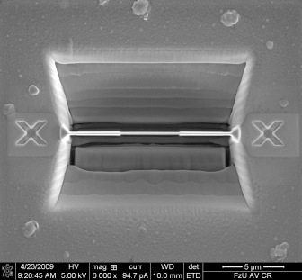
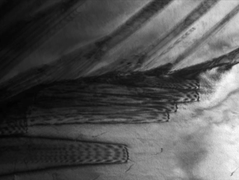
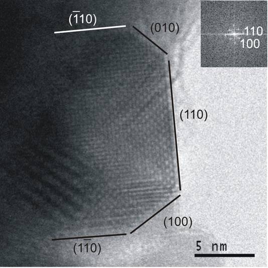
The difference between dark field and bright field observations is shown in the first picture. The second picture shows stress-induced martensitic transformation. This picture was taken during an in-situ experiment performed directly inside the microscope. During the experiment, a thin foil with fixation holes along its sides was subjected to deformation, and we could observe the development of the martensitic transformation. Consequently, in-situ experiments in combination with TEM allow us to observe the behaviour of materials subjected to deformation even at the atomic level such as the dislocation movement. The last picture shows an image taken by HRTEM (high resolution transmission electron microscopy). This technique enables the atomic-scale imaging, in this case of polycrystalline silicon with well discernible twin boundaries.
Diffraction mode
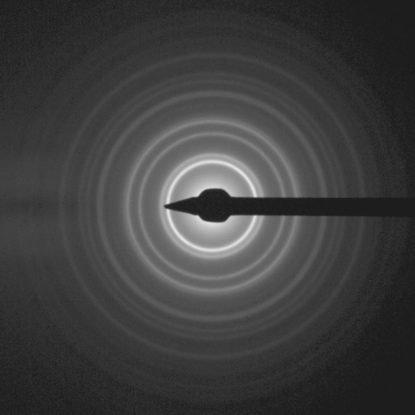
Transmission electron microscope can observe samples not only in the imaging mode (enabled by inelastic scattering of pass-through electrons), but also in the diffraction mode. Diffraction is caused by elastic scattering of passed-through electrons and their correlation. The data collected in the diffraction mode enable the determination of interplanar spacing, differences between amorphous and crystalline substances. Diffraction also enables the study of multi-phase materials and the identification of individual phases, as well as the determination of their interfaces and the defect analysis. Diffraction patterns (see the first picture) are very frequently used for indexing crystallographic planes. The diffraction mode is harder to grasp than the imaging mode; with a very demanding interpretation of results, requiring extensive knowledge of solid-state physics. When evaluating and subsequently interpreting the results, e.g. the CrysTBox software can be very helpful.
Secondary electrons and X-rays
In addition to pass-through electrons, the primary electron beam-sample interaction also results in X-rays and secondary electrons. In TEM, a spectrometry detector can be incorporated above the sample to analyse X-rays. It can either be an energy-dispersive X-ray spectrometer (EDS) or a wavelength-dispersive X-ray spectrometer. They can be used to determine chemical composition of a material.
Do you want to learn more? We highly recommend that you check a work by our colleagues from the Institute of Physics.