This website uses cookies so that we can provide you with the best user experience possible. Cookie information is stored in your browser and performs functions such as recognising you when you return to our website and helping our team to understand which sections of the website you find most interesting and useful.
Vyhledávání
Scanning electron microscope (SEM)
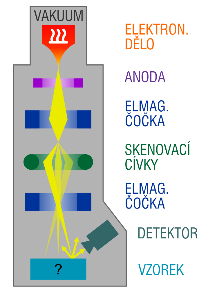
Scanning electron microscope (SEM), like the traditional microscope, is an optical instrument. Unlike traditional optical microscopes, this one, however, uses electrons instead of photons as a source of radiation and electromagnetic lenses instead of glass lenses. The entire internal space, the electron beam, and the sample are located in vacuum to prevent electrons from interacting with the atmosphere. The size of the sample is not specified exactly; with the main limiting factor being the size of the vacuum chamber used to insert the sample. The sample observed using SEM must be conductive, hence, to observe non-conductive materials, the sample needs to be covered with a layer of metallic powder (to be sputtered).
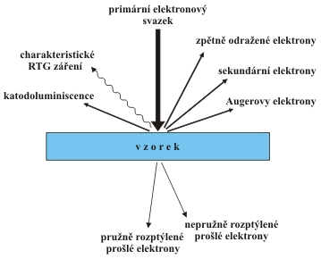
To study or analyse the surface of a sample, we use the electron beam-sample interactions to obtain a number of data on e.g. the sample’s microstructure, crystallographic ordering or chemical composition. To obtain the data, the microscope must be equipped with detectors to collect the information. In simple terms, typical data collected by SEM is the information that bounces back from the surface of the sample and from a small volume right under the surface (referred to as the interaction volume). The sample principle applies to Transmission Electron Microscope (TEM), which , unlike SEM, collects signals passing through the sample, allowing the study of the internal structure of a material.
Secondary electrons (SE)
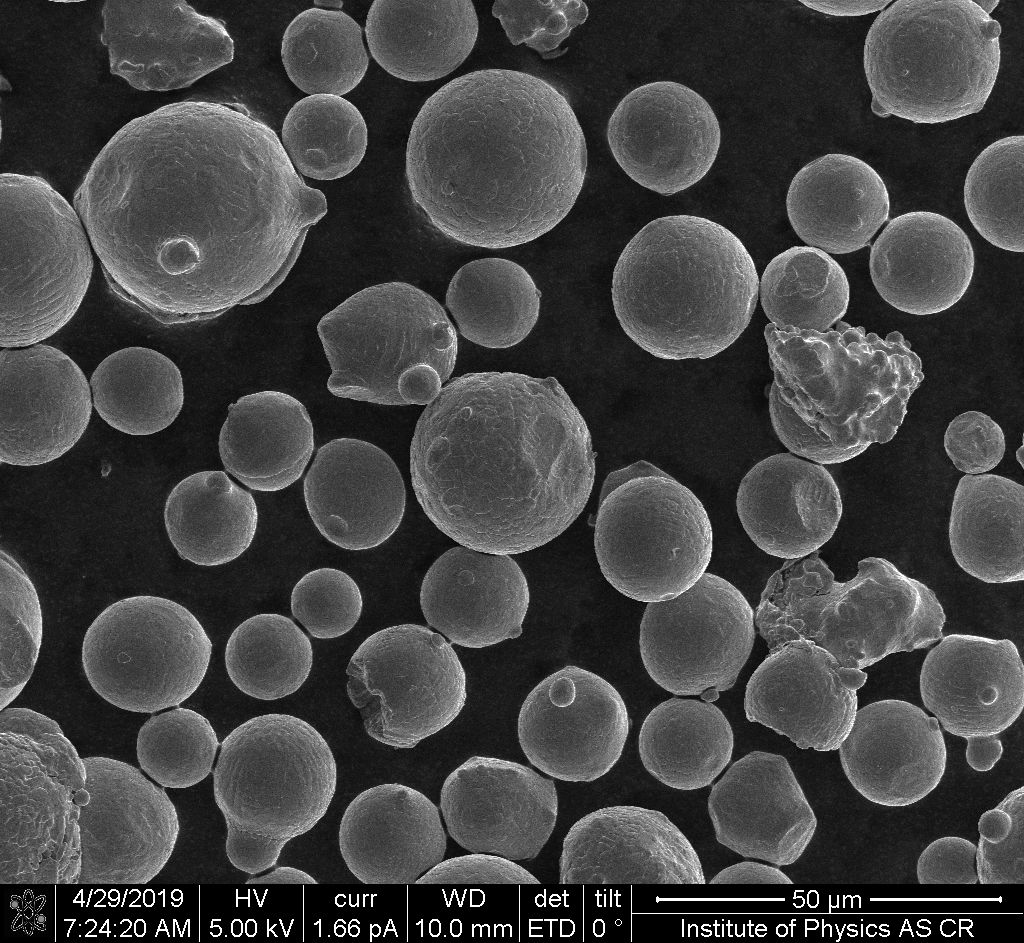
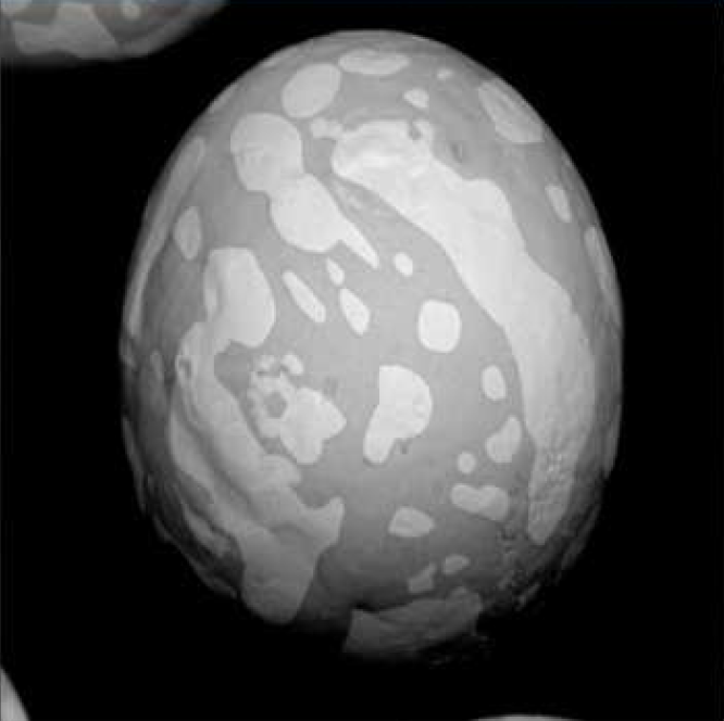
Secondary electrons (SE) are those generated directly from the place where the primary beam hit the surface or from a maximum of several nanometres under the surface. They carry information about the shape of the surface – the so called surface topography. Due to a great depth of field and a high resolution (given by the fact that electrons instead of photons are used, the wavelength of which is significantly shorter than that of the visible light), we use an image built up by processing secondary electron signals to analyse surfaces and structures or measure dimensions, e.g. of particles. As the secondary electrons are detected under certain angle to the surface of the sample, they appear on the image as lighter and darker spots, creating a 3D effect.
Back scattered electrons (BSE)
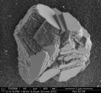
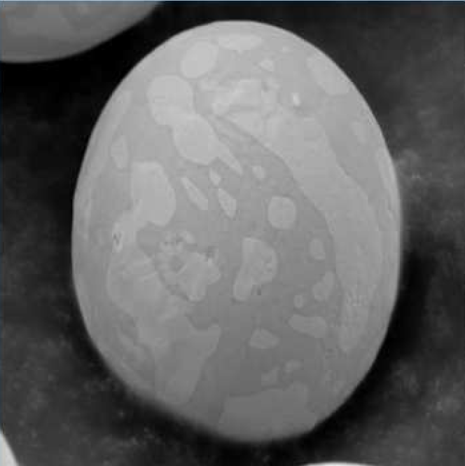
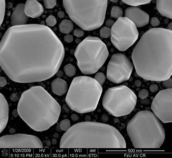
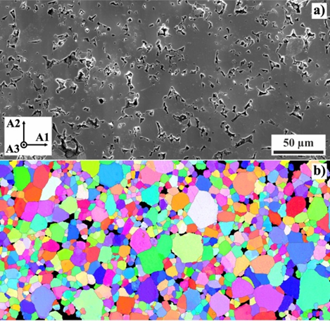
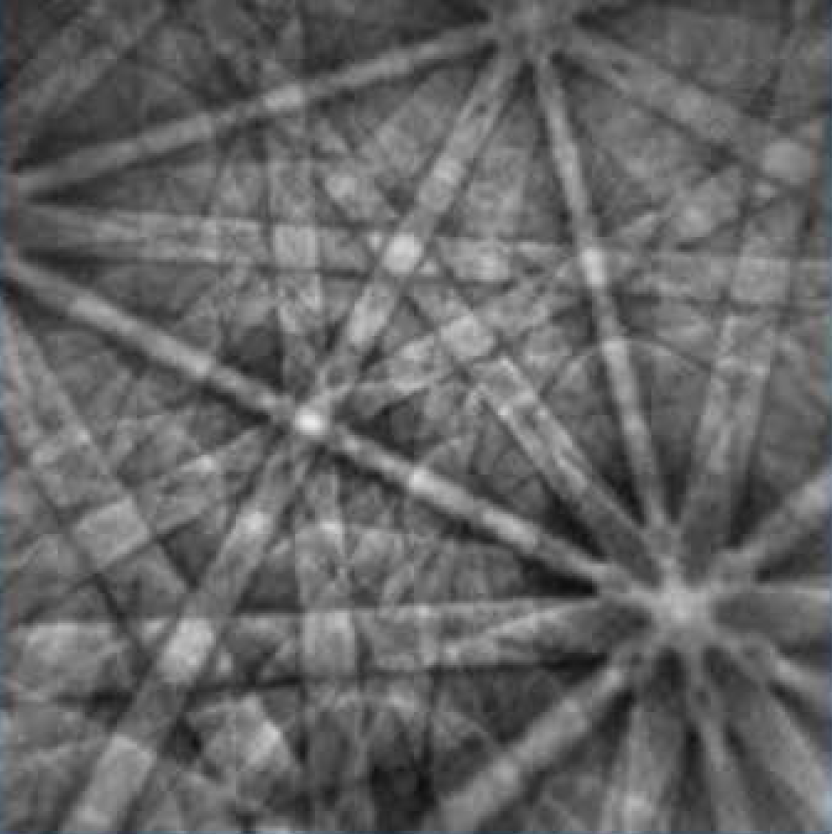
Back scattered electrons originate deeper (between tens to hundreds of nanometres) under the surface of the sample in the interaction volume than the secondary electrons, carrying information which is not only about the shape of the surface (topographical) but also about the type of the material; this is apparent from the first and the last image, if we observe the sample in the microscope’s image mode. The first figure shows golden particles on a carbon support. The marked contrast between the deposed particles and the support is caused by the big difference in both elements’ atomic numbers, i.e. the atomic number which is higher manifests itself in a lighter colour. Consequently, the contrast is not caused only by the surface topography, as with secondary electrons, but also by individual elements contained in the material. The difference between the observations of the same subject using secondary and back scattered electrons is clear from the last pictures in both categories. Back scattered electrons also enable the observation of a sample using a diffraction mode. This mode provides us with information on a material’s crystallography, i.e. on lattice plane orientation and lattice parameters, which can be visualized in colour maps (see the second picture, prepared using the EBSD method) or in the so called Kikuchi patterns (third picture).
X-ray radiation
Another type of signal we obtain from the impact of the primary electron beam on the sample are X-rays. This signal originates at a maximum depth of several microns under the surface within the interaction volume, and provides us, depending on the detectors used, with qualitative and quantitative information about the chemical composition of the material, the so called elements’ spectra (the elemental composition of a studied material). For the detection of characteristic X-rays, we can use EDS detectors (energy-dispersive X-ray spectroscopy) or WDS (Wavelength-dispersive X-ray spectroscopy). The difference between the two is significant. While using the WDS, we analyse element after element based on a characteristic X-ray wavelength, while using the EDS, we analyse the entire irradiated spectrum. This implies that the EDS method is significantly faster but its speed is reclaimed with lower precision and higher detection limits (in the orders of tenths of percent of an element’s mass content ), whereas the WDS is relatively lengthy, but very precise, with the detection limits ranging in the orders of hundredths of percent of the element’s content. More about EDS >>
Cathodoluminescence and Auger electrons
A special case with signal detection occurs with cathodoluminescence and Auger electrons. While cathodoluminescence enables the observation of a realistic colour image, because the process works with the visible light generated by the interaction of the primary beam with the sample, Augers electrons enable the elemental analysis of a material. Augers electrons are created during the transition of electrons from higher energy levels to a vacancy, releasing a certain an energy quantum. This energy can be irradiated in the form of a photon (characteristic X-ray) or passed on to an electron in the outer shell, giving the electron enough energy to leave the atom; resulting in the emission of the so called Auger electron. Auger electrons frequently occur with lighter elements such as carbon, nitrogen or boron.
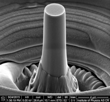
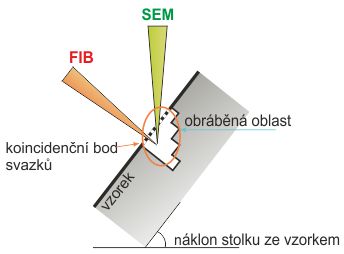
Focused ion beam (FIB)
A special type of the SEM microscope is a double-beam microscope which, in addition to a primary electron beam, uses a focused ion beam called the SEM-FIB microscope. This setup, which is schematically shown in figure 1, enables the micromachining of observed samples using a directed ionized atom flux. It is suitable for the preparation of foils for the transmission electron microscope, as well as for the in situ experiments using a microscope equipped with a nanoindenter. To get a better idea, the experiment starts by selecting an FIBem frame in a specific location, for example in a grain phase in the material. The frame can then be pulled or bent using a nanoindentor for us to observe the changes that occur, and to determine directly the basic mechanical properties of the given phase.
Do you want to learn more? We highly recommend that you check a work by our colleagues from the Institute of Physics.